Posts Tagged ‘Graphene’

From graphene to borophene

January 29, 2014

Technology development waves

The discovery of graphene is leading to a new excitement in materials research. I have a notion that technology advances take place in step waves, where each step is both enabled and constrained by the materials available. Each time a new material (or material family is discovered), technology development starts very fast and then tapers off until another material comes along and ignites a new development wave.

Boron is Carbon’s neighbour in the periodic table and the discovery of graphene has ignited studies to see if a similar variation of boron would be possible.

Boron is a Group 13 element that has properties which are borderline between metals and non-metals (semimetallic). It is a semiconductor rather than a metallic conductor. Chemically it is closer to silicon than to aluminium, gallium, indium, and thallium. Crystalline boron is inert chemically and is resistant to attack by boiling HF or HCl. When finely divided it is attacked slowly by hot concentrated nitric acid.

Boron, Symbol: B, Atomic number: 5, Atomic weight: 10.811, solid at 298 K

“Boron has one fewer electron than carbon and as a result can’t form the honeycomb lattice that makes up graphene. For boron to form a single-atom layer, theorists suggested that the atoms must be arranged in a triangular lattice with hexagonal vacancies — holes — in the lattice.”

A new paper shows that borophene is possible – now it just has to be made!

Zachary A. Piazza, Han-Shi Hu, Wei-Li Li, Ya-Fan Zhao, Jun Li, Lai-Sheng Wang.Planar hexagonal B36 as a potential basis for extended single-atom layer boron sheetsNature Communications, 2014; 5 DOI: 10.1038/ncomms4113

Brown University Press Release:

Unlocking the secrets of the B36 cluster
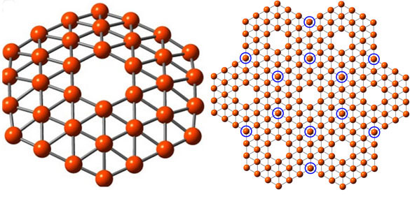
A 36-atom cluster of boron, left, arranged as a flat disc with a hexagonal hole in the middle, fits the theoretical requirements for making a one-atom-thick boron sheet, right, a theoretical nanomaterial dubbed “borophene.” Credit: Wang lab/Brown University

Graphene, a sheet of carbon one atom thick, may soon have a new nanomaterial partner. In the lab and on supercomputers, chemical engineers have determined that a unique arrangement of 36 boron atoms in a flat disc with a hexagonal hole in the middle may be the preferred building blocks for “borophene.”

Researchers from Brown University have shown experimentally that a boron-based competitor to graphene is a very real possibility.

Lai-Sheng Wang, professor of chemistry at Brown and his research group, which has studied boron chemistry for many years, have now produced the first experimental evidence that such a structure is possible. In a paper published on January 20 in Nature Communications, Wang and his team showed that a cluster made of 36 boron atoms (B36) forms a symmetrical, one-atom thick disc with a perfect hexagonal hole in the middle.

“It’s beautiful,” Wang said. “It has exact hexagonal symmetry with the hexagonal hole we were looking for. The hole is of real significance here. It suggests that this theoretical calculation about a boron planar structure might be right.”

It may be possible, Wang said, to use B36 basis to form an extended planar boron sheet. In other words, B36 may well be the embryo of a new nanomaterial that Wang and his team have dubbed “borophene.”

“We still only have one unit,” Wang said. “We haven’t made borophene yet, but this work suggests that this structure is more than just a calculation.” ……..

Wang’s experiments showed that the B36 cluster was something special. It had an extremely low electron binding energy compared to other boron clusters. The shape of the cluster’s binding spectrum also suggested that it was a symmetrical structure. ……..

…… That structure also fits the theoretical requirements for making borophene, which is an extremely interesting prospect, Wang said. The boron-boron bond is very strong, nearly as strong as the carbon-carbon bond. So borophene should be very strong. Its electrical properties may be even more interesting. Borophene is predicted to be fully metallic, whereas graphene is a semi-metal. That means borophene might end up being a better conductor than graphene.

“That is,” Wang cautions, “if anyone can make it.”

AbstractBoron is carbon’s neighbour in the periodic table and has similar valence orbitals. However, boron cannot form graphene-like structures with a honeycomb hexagonal framework because of its electron deficiency. Computational studies suggest that extended boron sheets with partially filled hexagonal holes are stable; however, there has been no experimental evidence for such atom-thin boron nanostructures. Here, we show experimentally and theoretically that B36 is a highly stable quasiplanar boron cluster with a central hexagonal hole, providing the first experimental evidence that single-atom layer boron sheets with hexagonal vacancies are potentially viable. Photoelectron spectroscopy of B36 reveals a relatively simple spectrum, suggesting a symmetric cluster. Global minimum searches for B36 lead to a quasiplanar structure with a central hexagonal hole. Neutral B36 is the smallest boron cluster to have sixfold symmetry and a perfect hexagonal vacancy, and it can be viewed as a potential basis for extended two-dimensional boron sheets.

The never ending wonders of Carbon

January 27, 2011

Not just all life as we know it and coal and diamonds and graphite and carbon nanotubes and now the new wonder-world of  graphene.

Carbon also has the highest melting and sublimation point of all elements. At atmospheric pressure it has no melting point as its triple point is at 10.8 ± 0.2 MPa and 4600 ± 300 K, so it sublimates at about 3900 K.

File:Carbon basic phase diagram.png

Theoretical phase diagram of carbon: Wikipedia

Evidence is mounting that a new crystal form of carbon – body-centered tetragonal (bct) – something between diamond and graphene must exist. Simulations show that it must. It is now up to experimentalists to prove it.

Image: From "Ab Initio study of the formation of transparent carbon under pressure," by Xiang-Feng Zhou et al., in Physical Review B, Vol. 82, No. 13; October 29, 2010

From Scientific American:

Now evidence is mounting that there is yet another crystal structure to add to carbon’s catalogue of wonders: a material that could find applications in mechanical components whose hardness varies depending on the pressure to which they are exposed.

This new type of carbon was first observed in 2003, when researchers placed graphite, a stacking of chicken-wire-shaped networks of carbon atoms, under high pressure at room temperature. Under this “cold” compression, the graphite began to assume a hybrid form, between that of graphene and of diamond, but its exact nature was unknown.

Two computer simulation studies now suggest that cold-compressed graphite contains crystals of a structure called body-centered tetragonal, or bct, in addition to another type called M carbon. In bct, groups of four atoms are arranged in a square. The squares are stacked in an offset manner, and each square forms chemical bonds with four squares in the layers above and four below. A team led by Hui-Tian Wang of Nankai University in Tianjin, China, showed that during cold compression the transition to bct carbon results in a release of energy, which means it is likely to happen in the real world.

A Japanese and American team also conducted a simulation in which bct carbon produced x-ray patterns similar to those seen in the 2003 study. …. Whether bct carbon exists or can be synthesized in its pure form “is still a task for experimentalists to test.” 

Now fluorographene from Graphene Nobel winners

November 9, 2010

A new paper by the Graphene Nobel winners in the Journal Small:

Fluorographene: A Two-Dimensional Counterpart of Teflon, by Rahul R. Nair, Wencai Ren, Rashid Jalil, Ibtsam Riaz, Vasyl G. Kravets, Liam Britnell, Peter Blake, Fredrik Schedin, Alexander S. Mayorov, Shengjun Yuan, Mikhail I. Katsnelson, Hui-Ming Cheng, Wlodek Strupinski, Lyubov G. Bulusheva, Alexander V. Okotrub, Irina V. Grigorieva, Alexander N. Grigorenko, Kostya S. Novoselov, Andre K. Geim. Article first published online: 4 NOV 2010, DOI: 10.1002/smll.201001555

Abstract

A stoichiometric derivative of graphene with a fluorine atom attached to each carbon is reported. Raman, optical, structural, micromechanical, and transport studies show that the material is qualitatively different from the known graphene-based nonstoichiometric derivatives. Fluorographene is a high-quality insulator (resistivity >1012Ω) with an optical gap of 3 eV. It inherits the mechanical strength of graphene, exhibiting a Young’s modulus of 100 N m−1 and sustaining strains of 15%. Fluorographene is inert and stable up to 400 °C even in air, similar to Teflon.

Graphane crystal. This novel two-dimensional material is obtained from graphene (a monolayer of carbon atoms) by attaching hydrogen atoms (red) to each carbon atoms (blue) in the crystal. (Credit: Mesoscopic Physics Group, Prof. Geim - University of Manchester)

Science Daily. University of Manchester scientists have created a new material which could replace or compete with Teflon in thousands of everyday applications. Professor Andre Geim, who along with his colleague Professor Kostya Novoselov won the 2010 Nobel Prize for graphene — the world’s thinnest material, has now modified it to make fluorographene — a one-molecule-thick material chemically similar to Teflon.

Fluorographene is fully-fluorinated graphene and is basically a two-dimensional version of Teflon, showing similar properties including chemical inertness and thermal stability. Teflon is a fully-fluorinated chain of carbon atoms. These long molecules bound together make the polymer material that is used in a variety of applications including non-sticky cooking pans. The Manchester team managed to attach fluorine to each carbon atom of graphene. To get fluorographene, the Manchester researchers first obtained graphene as individual crystals and then fluorinated it by using atomic fluorine. To demonstrate that it is possible to obtain fluorographene in industrial quantities, the researchers also fluorinated graphene powder and obtained fluorographene paper.

Fluorographene turned out to be a high-quality insulator which does not react with other chemicals and can sustain high temperatures even in air.

Industrial scale production of fluorographene is not seen as a problem as it would involve following the same steps as mass production of graphene. The Manchester researchers believe that the next important step is to make proof-of-concept devices and demonstrate various applications of fluorographene. Professor Geim added: “There is no point in using it just as a substitute for Teflon. The mix of the incredible properties of graphene and Teflon is so inviting that you do not need to stretch your imagination to think of applications for the two-dimensional Teflon. The challenge is to exploit this uniqueness.”


Graphene: Urban legend in the making?

October 8, 2010

As I posted earlier, the Nobel Prize in Physics 2010 was awarded jointly to Andre Geim and Konstantin Novoselov “for groundbreaking experiments regarding the two-dimensional material graphene”

It seems there is no controversy that “the first graphene samples formed were produced by pulling atom thick layers from a sample of graphite using sticky tape”.

But whether the graphite sample was actually lead flakes from a pencil and whether the sticky tape was actually Scotch tape is more uncertain. Nevertheless, it is now the stuff of urban legend and the subject of cartoons.


Nobel physics 2010.png

sticky tape + pencil = graphene


http://blogs.nature.com/strippedscience/2010/10/06/nobel-prize-in-physics-2010-catoon

Physics Nobel for graphene

October 5, 2010

What I thought might be the subject area of the Chemistry Nobel was in fact rewarded with the Physics Nobel prize today.

The Nobel Prize in Physics 2010 was awarded jointly to Andre Geim and Konstantin Novoselov “for groundbreaking experiments regarding the two-dimensional material graphene”

BBC: Andrei Geim and Konstantin Novoselov, both at Manchester University, UK, took the prize for research on graphene. Geim, 51, is a Dutch national while Novoselov, 36, holds British and Russian citizenship. Both are natives of Russia and started their careers in physics there.

Andre Geim

Andre Geim: Wikipedia

Graphene is a flat sheet of carbon just one atom thick; it is almost completely transparent, but also extremely strong and a good conductor of electricity. It consists of a hexagonal array of sp2-bonded carbon atoms, just like those found in bulk graphite. 2D materials display very interesting properties, and are fundamentally different from the 3D materials we encounter everyday. The discovery of 2D materials means that scientists now have access to materials of all dimensionalities, including 0D (quantum dots, atoms) and 1D (nanowires, carbon nanotubes).

Geim and Novoselov first isolated the fine sheets of graphene from graphite. A layer of graphite one millimetre thick actually consists of three million layers of graphene stacked on top of one another. The layers are weakly held together and are therefore fairly simple to tear off and separate. The researchers used ordinary sticky tape to rip off thin flakes from a piece of graphite. Then they attached the flakes to a silicon plate and used a microscope to identify the thin layers of graphene among larger fragments of graphite and carbon scraps.

Graphene can be used for many different purposes including transistors, gas sensors, support membranes for TEM and inert transparent coatings.

Konstantin Novoselov

Konstantin Novoselov : Photo: University of Manchester, UK

It provides the possibility for further research in quantum physics, relativity and has allowed the Klein paradox to be observed for the first time.

Some scientists have precicted that graphene could one day replace silicon – which is the current material of choice for transistors. It could also yield incredibly strong, flexible and stable materials and find uses in transparent touch screens or solar cells.

Ten years ago, Professor Geim and Professor Sir Michael Berry from the University of Bristol were jointly awarded an Ig Nobel prize for their experiments using magnetic fields to levitate live frogs.

Graphene Ultracapacitors

September 27, 2010

Graphene is very much the material of the moment.

But graphene actually dates back to 1961. Hanns-Peter Boehm and coauthors Clauss, Fischer, and Hofmann isolated and identified single graphene sheets by transmission electron microscopy (TEM) and X-ray diffraction in 1961 and authored the IUPAC (International Union of Pure and Applied Chemistry) report formally defining the term graphene in 1994. He must have been surprised to learn of its discovery in 2004.

Graphene is a flat monolayer of carbon atoms tightly packed into a two-dimensional (2D) honeycomb lattice, and is a basic building block for graphitic materials of all other dimensionalities. It can be wrapped up into 0D fullerenes, rolled into 1D nanotubes or stacked into 3D graphite.

“Electrons in graphene, obeying a linear dispersion relation, behave like massless relativistic particles. This results in the observation of a number of very peculiar electronic properties – from an anomalous quantum Hall effect to the absence of localization – in this, the first two-dimensional material. It also provides a bridge between condensed matter physics and quantum electrodynamics, and opens new perspectives for carbon-based electronics.” (M.I. Katsnelson)

Properties of graphene are still being discovered and are leading to new studies of relativity and a wave of potential applications in physics, electronics, chemistry and biology (transistors, gas molecule detection, nano-ribbons, nano-tubes, bio-devices and transparent electrodes).

graphene-structure

graphene-structure:www.thp.uni-koeln.de/graphene08/

The IEEE reports that the ultracapacitor—the battery’s quicker cousin—just got faster and may one day help make portable electronics a lot smaller and lighter.  John Miller, president of the electrochemical capacitor company JME, in Shaker Heights, Ohio, and his team reported the new ultracapacitor design this week in Science.

Ultracapacitors don’t store quite as much charge as batteries but can charge and discharge in seconds rather than the minutes batteries take. Using nanometer-scale fins of graphene, the researchers built an ultracapacitor that can charge in less than a millisecond. This agility, its designers say, means that the devices could replace the ubiquitous bulky capacitors that smooth out the ripples in power supplies to free up precious space in gadgets and computers.

ultracapacitor cell: venturebeat.com

One team member, Ron Outlaw, a material scientist at the College of William and Mary, in Williamsburg, Va., came up with an electrode consisting of up to 4 sheets of graphene —a one-atom-thick form of carbon with unusual electronic properties. The graphene was formed so that it stuck out vertically from a 10-nanometer-thick graphite base layer.

Miller’s team, which also included Brian Holloway, a program manager at the Defense Advanced Research Projects Agency (DARPA), tested its graphene ultracapacitor in a filtering circuit, part of an AC rectifier. Many rectifiers leave a slight AC echo behind, called a “voltage ripple,” and it’s the capacitor’s job to smooth it out. In order to do that, the capacitor needs to respond well at double the AC frequency—120 hertz in the United States. Most commercial ultracapacitors fail at this filtering role at around 0.01 Hz, but when Miller’s team tested its ultracapacitor in such a 120-Hz filtering circuit, it did the job. That means the smaller ultracapacitors could replace the big electrolytic capacitors that do the filtering now. Miller estimates that a commercial version, operating at 2.5 volts, could be less that one-sixth the size of any other 120-Hz filtering technology.

But even if graphene proves to be more promising than carbon nanotubes, silicon isn’t going away anytime soon.


%d bloggers like this: