I have been amazed at the stupidity of the European response to Trump’s rhetoric about Greenland. They seem to have no clue as to the game that is being played. While Trump is negotiating they are reacting to tactics and red herrings and have no idea what the end goal is and even which game is being played. It is not that Trump is conferring idiocy upon the clueless European leaders – they have been self-harming themselves!
For the US (Trump) the motive in both regions is not personal pique or detest for Maduro. It is not either about resources for just their own sake. This is part of the Great Game between the US and China for the coming 100 years. It is about strategic leverage against China’s growing global footprint. That is the thread tying them together. In another century it was the Great Britain and Russia. The US and China are taking the Great Game to new regions. The serious geo-political analysts see it. I am afraid that the European leaders get bogged down and utterly distracted by Trump’s injection of red herrings which they just cannot discern.
Venezuela – Yes oil but not only oil
Venezuela’s primary strategic value is its natural resources, above all oil. It has the world’s largest proven oil reserves. The recent U.S. intervention and pressure campaign explicitly cites oil access and disruption of adversarial influence as motives.
- China has deep financial and commercial ties with Venezuela, long providing loans and buying Venezuelan energy and commodities.
- Venezuelan rare earths and critical minerals are potential future assets — but currently underdeveloped, lacking infrastructure and clear exploitation plans.
The U.S. objectives are no secret and have been discussed so openly that I wonder why reporters of the lower kind and one-note politicians so easily forget.
- Deny China Easy Access to Resources
Even if Venezuela isn’t a top rare-earth producer today, Washington sees value in preventing Beijing from locking up any potential resources or influence that could reduce U.S. leverage. This jibes with official U.S. rhetoric about countering “non-hemispheric competitors.” - Break China’s Growing Footprint in the Region
Latin America isn’t neutral territory anymore. China is a major trading partner across many states, and U.S. strategy now frames this as a geostrategic threat – something that could give Beijing leverage deep in the Western Hemisphere. - Strategic Oil Supply and Energy Security
Oil still matters as base strategic power: controlling Venezuelan oil limits Beijing’s access to energy markets, which could constrain China’s industrial or military trajectory in a crisis. - Supply Chain & Rare Earth Sentiment
Some U.S. policy thinkers argue the future of tech and defence depends on diversifying supply chains away from China – and Venezuela’s minerals could play into that if infrastructure and political stability were achieved.
My assessment is that the U.S. wants to disrupt Chinese access. This fits with how Washington/Rubio/Trump are now framing their moves. This is a long-term geo-political play about material resources and influence. A not insignificant part is the rare earths potential in Venezuela even if they are not yet a fully realized asset.
Greenland: Raw Materials and Strategic Geography
Greenland doesn’t fit exactly the same profile as Venezuela, but it does fit the same pattern. It is about access to strategic resources and a denial of geo-political access to China. Greenland hosts some of the richest deposits of rare earth elements outside China. U.S. strategic planners see this as a way — someday — to dilute China’s dominance in critical raw materials that power everything from electric vehicles to missiles. Besides minerals, Greenland is a gateway to the Arctic — territory increasingly contested by Russia and China. U.S. military interest there reflects broader strategic positioning. Rather than wait for China (or Russia) to embed itself economically or militarily, the U.S. has pushed aggressive diplomacy, investment deals, and even territorial rhetoric, explicitly meant to keep rival influence out.
Extracting rare earths in Greenland is currently expensive, technically difficult, and far from market scale. Greenland’s harsh climate and lack of infrastructure make mining a long-term project. But from a strategic viewpoint, that doesn’t matter much — the U.S. wants to lock in preferential access and preclude China from doing so first.
The Great Game: supply chain security
Both cases tie into a bigger story about critical minerals, supply chains, and great-power competition:
-
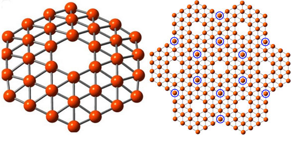
China still controls a vast share of refining and processing for rare earths and other minerals, not just mining.
-
The U.S. has made securing alternative sources, both domestic and allied, a declared priority, often written and described in the language of national security.
-
Latin America and the Arctic are the competitive regions for the next century where access to resources and influence matters as much as traditional military positioning.
- Within the next century new off-Earth regions of supply chain competition and security will be opening up with the moon (China present and US playing catch-up) and Mars (US first) already included within strategic planning
This not about gestures and virtue signalling and personal pique. It is plain and simple geopolitics.
Who is going to have control of critical raw materials and whose military or economic reach will have dominance in key regions?
That is the game being played not whether the Peace Prize can be legally shared or not!!
Afterword
U.S. actions in Venezuela and Greenland are partly about denying China access to strategic resources and partly about securing their own access:
-
Venezuela: important for oil access and preventing Chinese economic dominance in the hemisphere; rare earths are a secondary but growing part of that calculus.
-
Greenland: a long-range bet on critical materials, strategic geography, and preemptive advantage over China and Russia.
This is part of the Great Game between the US and China for the coming 100 years. It is about strategic leverage against China’s growing global footprint. That is the thread tying Venezuela and Greenland together.


, Chinese Premier")


